PCB design
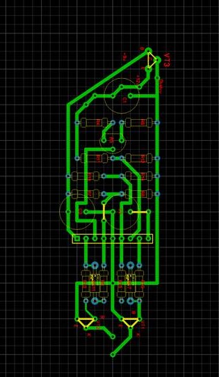
Proper circuit layout is the key to successful product operation
An incorrectly wired board will emit electromagnetic interference and will make it difficult or impossible to mount the components properly. Therefore, we follow the same rules for wiring printed circuit boards:
- In accordance with GOST and IPC requirements
- Performing work in the program P-CAD
- Define board type and pad sizes correctly
- Correctly placing components on the board
Cost
The cost of developing a printed circuit board is determined individually. Because depends on the complexity of the product:
- number of PCB layers (maximum 8 layers)
- number of pins of electronic components included in the product specification